These days I use DesignSpark PCB for designing my PCBs. A few years ago, I judged it to be the best of the free software after trying Eagle, Kicad and others – and I like the way that RS is continuously developing it. Ultimately though, whatever CAD tool you choose, the most important thing is to become familiar with it.
I used DesignSpark to generate a PCB for my vibrating wristband from the schematic that I had already captured. I manually positioned the components, but let the auto-router route all the tracks. I had to move the components slightly over a few iterations to get the auto-router to be able to complete all the nets.  I have previously had two sets of PCBs made at ITEAD Studio, and been very happy with the results. Certainly their prices are good at $1 per 5cmx5cm board.
Just be aware of minimum sizes in your design. In the past I have specified silkscreen text and lines that were too small to be printed. It is very easy to lose touch of just how small things really are when you are looking at a full screen CAD view. ITead has posted guidelines here, but basically you should be fine if you don’t need to go below 0.2 mm.
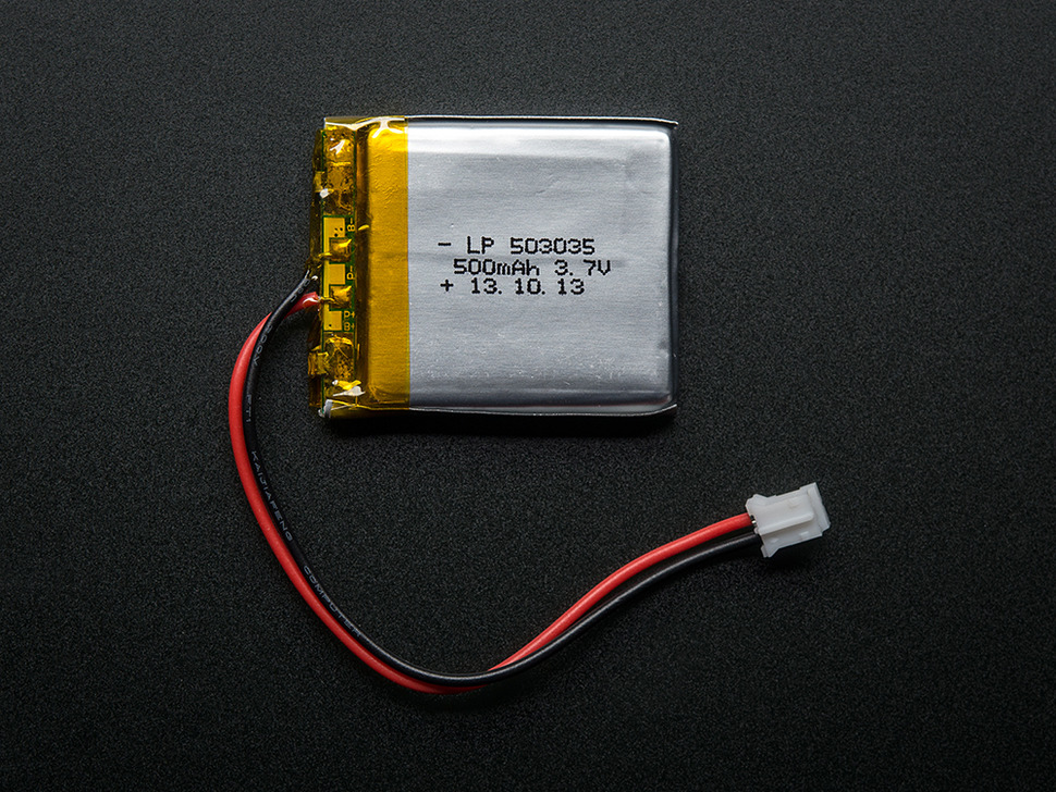 I designed the board with exactly the same dimensions as the Adafruit battery that I plan to use, since the board will sit on top of this battery (37mm x 30mm). The process for generating the correct files for an ITEAD Studio 2-layer board is quite simple, but you should follow the following steps once you have finished your design:
Choose the menus Output|Manufacturing Plots from within DesignSpark
Tick the following…
-
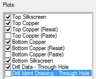 Top Silkscreen
 - Top Copper
- Top Copper (Resist)
- Bottom Copper
- Bottom Copper (Resist)
- Bottom Silkscreen
- Drill Data – Through Hole

Add a new Outline plot
- Select button Add Plot..
- Choose Gerber
- Rename Plot Name to Outline
- Change Plot Type to Outline
- Choose Layers Tab
- Set [Board Outline] “Selected” to Y
 Select Drill Data – Through Hole
- Choose Output Tab | Device Setup
- Untick Separate Files for Plated and Unplated holes
Click “Run”
Delete the .txt and .mop files, as these aren’t needed
Rename output files to the following extensions:
- Top Silkscreen: pcbname.GTO
- Top Copper: pcbname.GTL
- Top Copper (Resist): pcbname.GTS
- Bottom Copper: pcbname.GBL
- Bottom Copper (Resist): pcbname.GBS
- Bottom Silkscreen: pcbname.GBO
- Outline: pcbname.GKO
- Drill Data – Through Hole: pcbname.TXT
Zip these Gerber files into one file (per design): pcbname.ZIP
 Send Gerber files to [email protected] and place the order number (that you would have been sent) in the e-mail subject,
[Update]: Itead now has a system to upload your files directly to their website, as described in their Self-help PCB Service Instruction.
I have not experienced any problems after following this process, but you would probably want to check that the output files look correct before submitting. To do this, I found an excellent open source Gerber viewer at http://sourceforge.net/projects/gerbv/
You open the 6 Gerber files in Gerbv, which enables you to view each layer separately or superimposed: 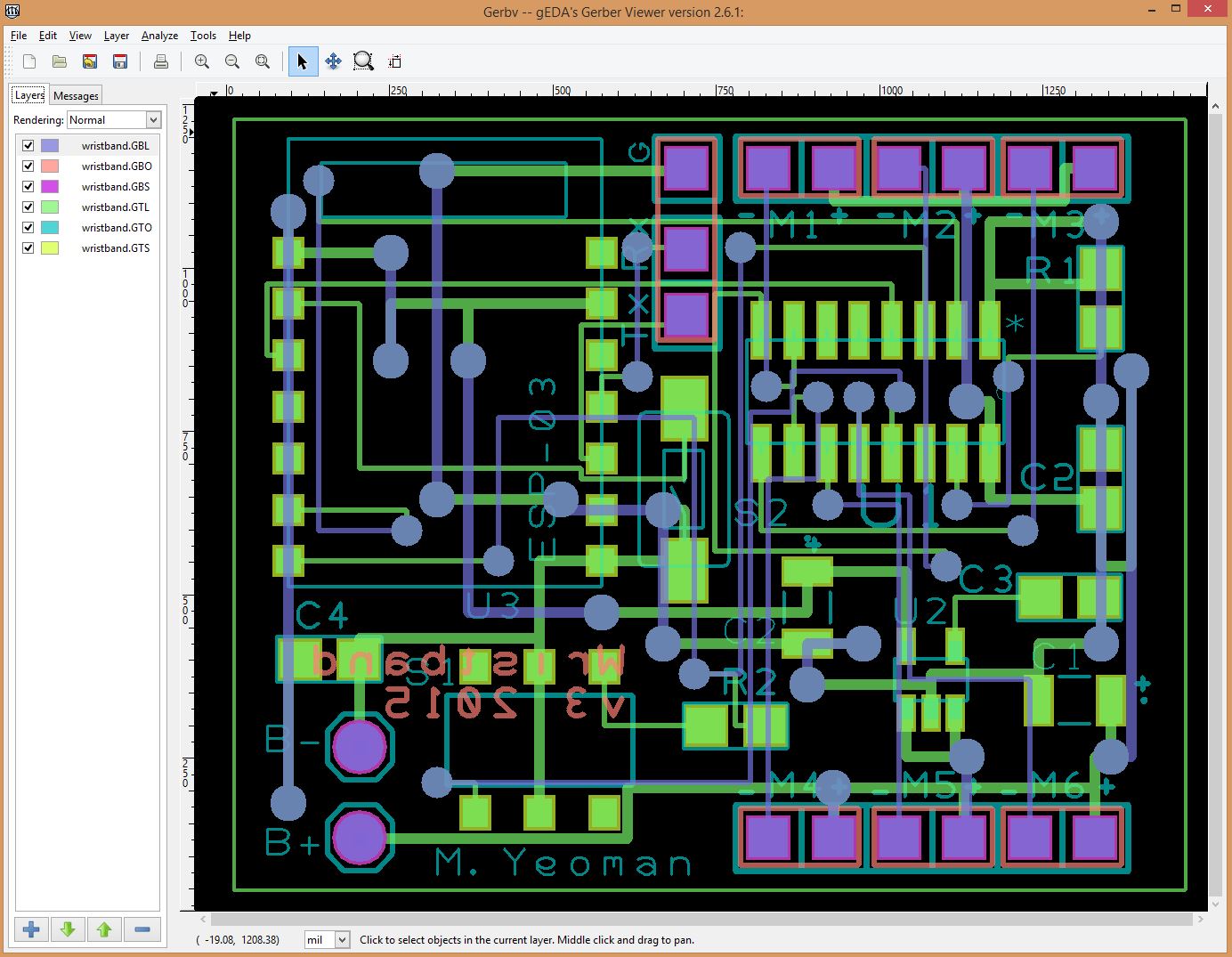 I’ll post a photo of the resulting boards when they come back… which will be only in several weeks as I picked the lowest cost shipping option.
Gives me time to work on the software.. more on that next week!
Reblogged this on bits4bots and commented:
Nice 🙂